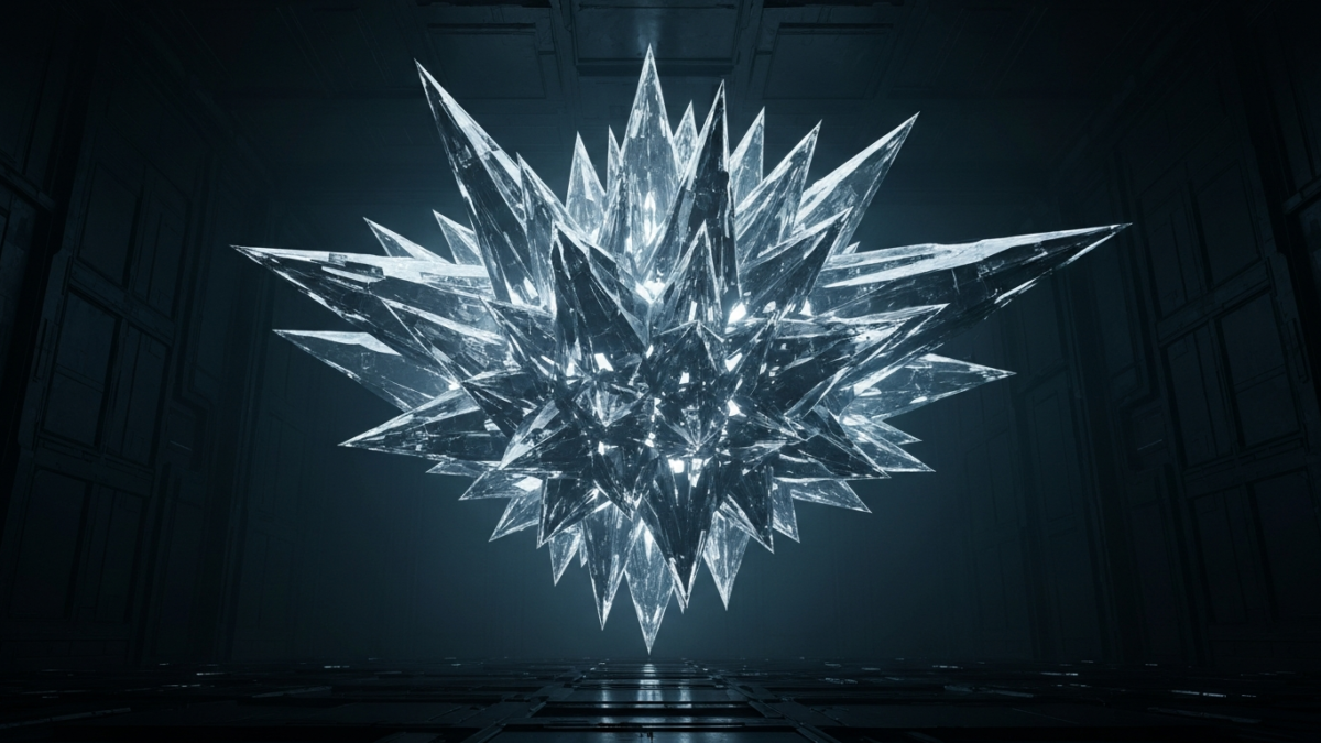
NVIDIA is officially moving beyond the realm of gaming frames and into the heart of hardcore material science. As the official NVIDIA documentation announced, and as reported by NVIDIA, the tech giant has unveiled its Accelerated X-ray Analysis for Nanoscale Imaging (XANI) workflow. This breakthrough leverages the massive power of 32 NVIDIA GB200 Grace Blackwell Superchips to perform tasks that were previously deemed impossible for real-time applications. By shrinking the processing time for 42 terabytes of data from a staggering nine months down to less than four hours, NVIDIA is effectively giving scientists a time machine. This level of compute is critical for the development of next-generation hardware, including the advancements we are seeing in the 2026 battery battle where material endurance is everything.
The XANI project has already seen adoption across a wide spectrum of scientific communities, ranging from quantum physics to materials chemistry. By utilizing CUDA Python and distributed computing, the team demonstrated a 1,000x speedup when scaling to 64 GPUs. This isn’t just about raw speed; it is about the precision of acquired data being preserved while the I/O throughput sees a 165x acceleration. As we question PlayStation’s AI ambition and the ethical lines of massive compute, NVIDIA is showing that the Blackwell architecture is the undisputed king of the exascale era.
The Breakdown
- Hardware Specs: The workflow utilizes 32 NVIDIA GB200 Grace Blackwell Superchips, featuring 186 GB HBM3e, four 200 Gb/s storage NICs, four 400 Gb/s compute NICs, and two 480 GB RAM per node.
- Massive Data Handling: XFEL facilities generate data at megahertz rates, producing up to 1 million shots per second with 35-million-pixel cameras, resulting in hundreds of terabytes to petabytes of information.
- Processing Revolution: Computational time for 42 TBs of data was reduced from nine months to under four hours, maintaining full precision using the cuPyNumeric distribution engine.
- Global Research Facilities: The XANI workflow is designed for use at SwissFEL in Switzerland, SACLA in Japan, LCLS-II at SLAC, European XFEL in Germany, and PAL in Korea.
- Software Libraries: The acceleration is powered by cuPyNumeric, LMFIT, NumPy, SciPy, and a multithreaded version of Hierarchical Data Format 5 (HDF5).
- I/O Performance: Achieved 76 GB/second on a single node and 700 GB/second on 16 nodes using GPUDirect Storage (GDS), cuFile library, and the vfd-gds plugin.
- Data Layouts: The system supports contiguous, chunked, and virtual datasets (VDS) layouts to ensure efficient multidimensional reads across Lustre storage systems.
The Jay Respawns Take
While most of the world is looking at Blackwell and wondering how many extra rays it can trace in Cyberpunk 2077, the real story is how this hardware is fundamentally changing the speed of human discovery. We are talking about a 43x speedup on a single GPU compared to traditional CPU-bound pipelines. For gamers, this matters because the semiconductors and battery technologies being analyzed today are the ones that will power the RTX 60-series or the next Nintendo handheld. When you can iterate on material defects in four hours instead of nine months, the pace of hardware evolution hits warp speed.
It is also worth noting the sheer technical wizardry involved in bypassing the CPU entirely via GPUDirect Storage. By removing the host memory bottleneck, NVIDIA is proving that the GPU is no longer a co-processor; it is the center of the universe. The integration of CUDA Python into these workflows means that the barrier to entry for high-performance computing is dropping, even as the power ceiling explodes. This is the kind of “Fast & Meaty” tech update that reminds us why NVIDIA currently owns the conversation.
Stay tuned to Jay Respawns as we continue to track how Blackwell is reshaping the future of gaming and science.


Comments